
wafer grinding introduction
Global Wafer Grinder Market Trends Forecast to 2023 ...
Report Name: Global Wafer Grinder Consumption Market Report. The Worldwide Wafer Grinder Market is a recently published research report that covers every aspect of....
Solutions for thinning, dicing and packaging of power ...
Wafer edge after Z1axis grinding After Z1axis grinding After 15 µm lapping After 27 µm lapping Wafer edge after Z1axis grinding After Z1axis grinding After 30 µm lapping After 40 µm lapping Ultrasonic grinding makes the affected layer shallower, it decreases lapping removal amount Ø 34inch sapphire Ø#320 Z1axis grinding >Lapping...
Fine grinding of silicon wafers PDF Free Download
However, no published articles are available regarding fine grinding of silicon wafers. In this paper, the uniqueness and the special requirements of the silicon wafer fine grinding process are introduced first. Then some experimental results on the fine grinding of silicon wafers are presented and discussed....
Fine grinding of silicon wafers: a mathematical model for ...
50 Fine grinding of silicon wafers: a mathematical model for grinding 51 marks 52 S. Chidambaram a, ... Introduction 76 Silicon wafers and their manufacturing processes 77 Integrated circuits (ICs) are built on semiconductor 78 wafers. Over 90% of semiconductor wafers are silicon...
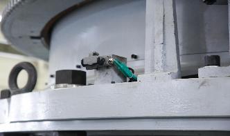
Mechanical Edge Grinding of SAW Wafers
groovewafer interface to flush grind debris from the groove and to eliminate heat buildup. 4) With bevel complete, the grind chuck moves away from the grind wheel and the beveled wafer is unloaded from the grind chuck with a vacuum cup and placed on a pair of parallel belts. These belts transfer the wafer to the receiving cassette. 5) When ......
Study on Structure Transformation of Si Wafer in Grinding ...
In this paper, the surface and subsurface of silicon wafers ground by different wheels have been studied. In the conventional grinding with diamond wheels, it is shown from the top that the subsurface of wafer consists of amorphous Si, followed by a thin damaged layer, strained crystal with a large compressive residue stress, and then the bulk material in single crystal....
Lecture 21: Silicon wafer manufacturing NPTEL
4 Wafer manufacturing 9 1 Introduction The rst step in integrated circuit (IC) fabrication is preparing the high purity single crystal Si wafer. This is the starting input to the fab. Typically, Si wafer refers to a single crystal of Si with a speci c orientation, dopant type, and resistivity (determined by dopant concentration). Typically, Si ......
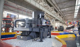
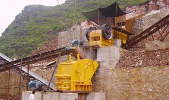
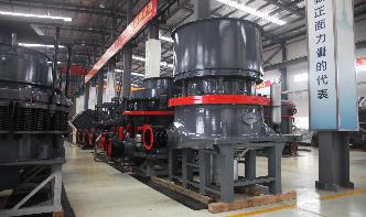
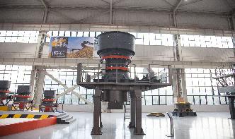
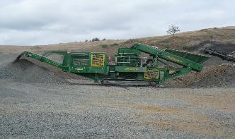
introduction about grinding machine pdf
Introduction of Wafer Surface Grinding Machine . Introduction of Product Introduction of Wafer Surface Grinding Machine Model GCG300 Junichi Y amazaki Meeting the market requirements for silicon wafers with high flatness and minimal damage, which have. Contact Supplier...
IRBased Temperature Measurement in Rotational .
The proof of concept for IRbased temperature measurement in rotational grinding of sapphire wafers was successfully achieved. Due to the limited detector frequency, the so called "background temperature" of the abrasive layer is measured. Highest temperatures of ....
grinding machine introduction
introduction of grinder machine Introduction Grinding Machine grinding mill equipment. The grinding machine consists of a bed with a fixture to guide and hold the work piece and a powerdriven grinding wheel spinning at the required speed Introduction to Machine Tool Frame The frame is a machine s fundamental element This casting or fabricated section carries ....
Finite element analysis for grinding and lapping of wire ...
68 The main issue with grinding of wiresawn wafers is UNCORRECTED PROOF 69 waviness, because conventional grinding process cannot 70 effectively remove waviness [9,10,14]. In the literature to 71 date, there are no reports on systematic study of this issue. 72 This paper, through a model of finite element analysis 73 (FEA), aims at providing insight on how waviness is...

The Global Semiconductor Wafer Polishing Grinding ...
May 29, 2019· The "Semiconductor Wafer Polishing and Grinding Equipment Global Market Outlook ()" report has been added to 's offering. According to ....
Grinding of silicon wafers: A review from historical ...
Extension of singleside wafer grinding from thinning (back grinding) of completed device wafers to flattening of substrate wafers is manifested by the history of wafer grinders at Disco Corporation, as shown in Table 1. Disco Corporation is a leading manufacturer of wafer grinders....
CiteSeerX — Grinding of silicon wafers: a review from ...
CiteSeerX Document Details (Isaac Councill, Lee Giles, Pradeep Teregowda): The majority of semiconductor devices are built on silicon wafers. Manufacturing of high quality silicon wafers involves several machining processes including grinding. This review paper discusses historical perspectives on grinding of silicon wafers, impacts of wafer size progression on applications of grinding in ......
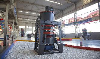
Introduction of Wafer Surface Grinding Machine Model ...
Introduction of Product Introduction of Wafer Surface Grinding Machine Model GCG300 Junichi Yamazaki Meeting the market requirements for silicon wafers with high flatness and minimal damage, which have become increasingly stringent in the face of highly integrated semiconductor devices, a fully automated surface grinding machine has been developed and introduced into the market, where it ....
introduction grinding machine
introduction to plate grinding machine Introduction of semiconductor wafer grinding machine. CYMP202B grinding/polishing machine is equipped with 8" lapping plate and can be used as a standard manual. grinder, or lapping/polishing machine for two pieces flat sample and....
IC Assembly Packaging PROCESS AND TECHNOLOGY
Back Grinding y Process to thin down the wafer from original thickness to the required final thickness by abrasive grinding wheel in combination to mechanical/chemical polish y Common industries used wafer thickness 815 mils (200300microns) y Current Machine capability mil (25microns) y ....